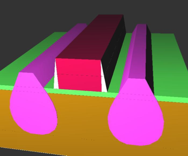
Our product suite includes advanced simulation tools designed to comprehensively model and optimize critical processes in electron beam lithography. These tools provide detailed insights into electron scattering dynamics, charging effects that can distort patterns, thermal impacts such as resist heating, precise energy deposition profiles, and the complex chemical and physical changes during resist development. By accurately simulating these phenomena, our software empowers users to enhance pattern fidelity, reduce defects, and accelerate process development for cutting-edge nanofabrication applications.
more
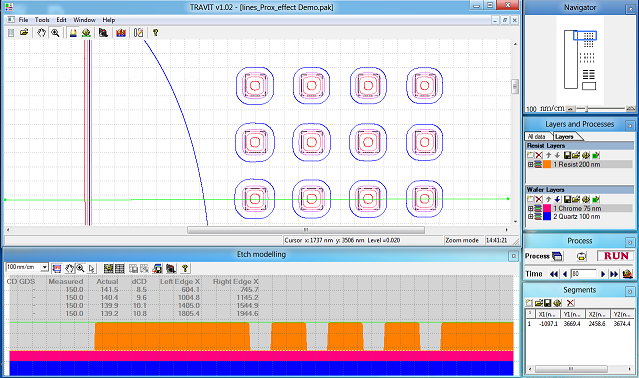
Our advanced software suite models and optimizes every stage of the electron beam lithography process. This includes detailed simulation of electron scattering and charging effects, placement errors due to proximity interactions, and thermal influences such as resist heating. Additionally, the software accurately predicts resist exposure profiles and simulates development behavior, enabling precise control over pattern fidelity. By accounting for these complex physical phenomena, our tools empower researchers and engineers to refine their lithographic processes, improve yield, and push the limits of nanoscale fabrication.
more
The SCATT software simulates optical scatterometry based on first-principles physics, relying on rigorous electromagnetic modeling to predict how light interacts with intricate surface structures at the micro- and nanoscale. By doing so, it provides a detailed understanding of how variations in fabrication parameters—such as feature dimensions, material properties, or layer thicknesses—affect the resulting optical signals. This allows users to analyze the sensitivity of measured data to specific process variations, helping identify which aspects of the manufacturing process most influence signal behavior. Additionally, SCATT assists in evaluating the applicability of scatterometry for inspecting particular layers or structures within a device, offering insights into which measurement configurations are best suited for achieving reliable, high-resolution results. Overall, the software serves as a powerful tool for both process development and metrology optimization in advanced semiconductor manufacturing.
more
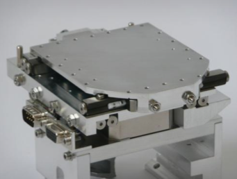
The company specializes in the fabrication of custom test chips tailored to specific experimental or production needs, while also offering a diverse selection of standard, off-the-shelf test chips for more general applications. These chips are available in a wide range of sizes, spanning from small-scale 5 mm formats up to full 300 mm wafers, accommodating a broad spectrum of testing environments and equipment compatibilities. In addition to chip manufacturing, the company develops advanced photonic components, including photonic structures directly imprinted onto the tips of optical fibers. This integration enables convenient and compact solutions for precise wavefront manipulation, facilitating alignment, beam shaping, and optical coupling in various photonics and sensing applications. more